Semiconductor Metrology & Inspection Equipment Market Size
| Study Period | 2018 - 2028 |
| Base Year For Estimation | 2022 |
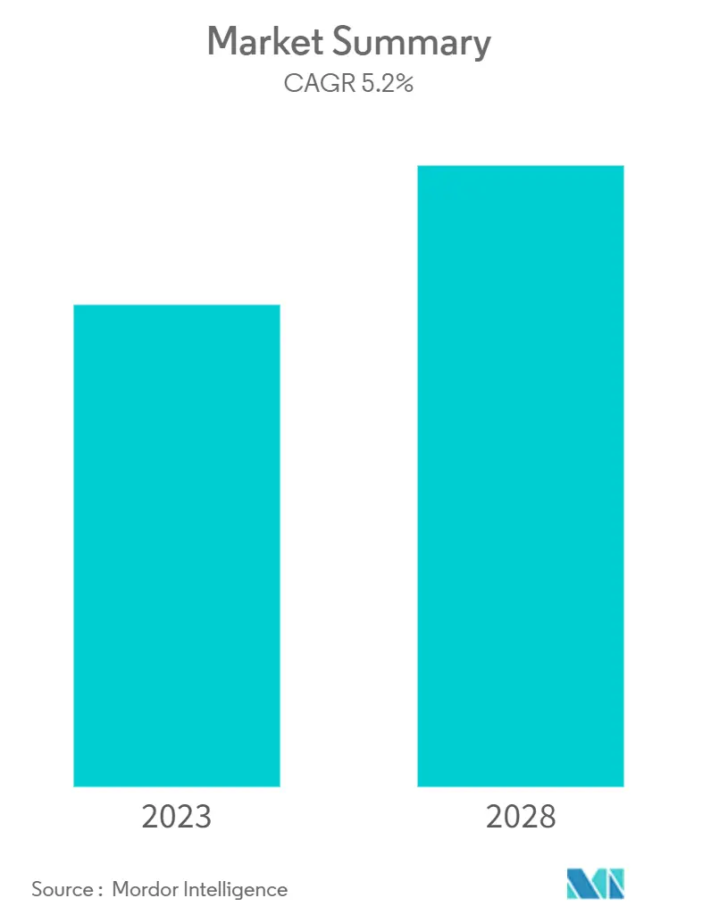
| CAGR | 5.20 % |
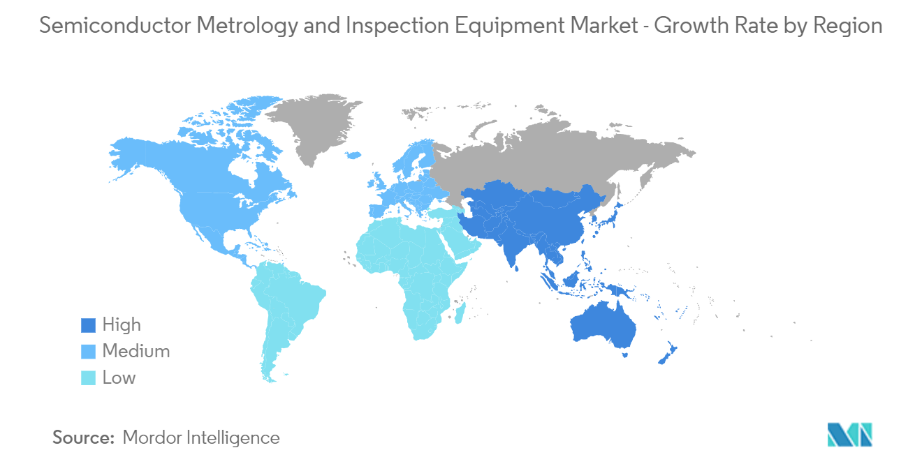
| Fastest Growing Market | Asia Pacific |
| Largest Market | Asia Pacific |
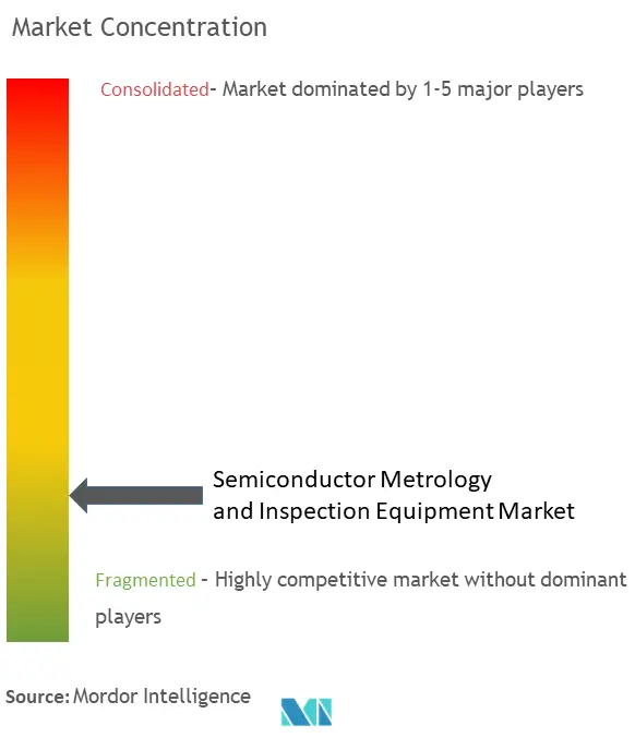
| Market Concentration | Low |
Major Players
*Disclaimer: Major Players sorted in no particular order |
Need a report that reflects how COVID-19 has impacted this market and its growth?
Semiconductor Metrology & Inspection Equipment Market Analysis
The semiconductor metrology and inspection equipment market size is expected to grow from USD 9.95 billion in 2023 to USD 12.82 billion by 2028 at a CAGR of 5.2% during the forecast period.
- Semiconductor metrology and inspection are essential for managing the semiconductor manufacturing process. There are 400 to 600 steps in the manufacturing process of semiconductor wafers, which are undertaken in one to two months. If deficiencies occur early in the process, all the work undertaken in the subsequent time-consuming steps will be wasted. Metrology and inspection processes are established at critical points of the semiconductor manufacturing process to ensure that a specific yield can be confirmed and maintained.
- Smartphones and other applications across consumer electronics and automotive applications are driving the demand for high-performance, low-cost semiconductor materials. These industries are inspired by technology transitions, such as wireless technologies (5G) and Artificial Intelligence. Also, the trend of increasing Internet of Things (IoT) devices is expected to force the semiconductor industry to invest in this equipment to attain smart products.
- The growing trend of adoption of connected devices in residential and industrial sectors augments the demand for high-performance semiconductors. According to a study by Metova, a provider of mobiles, connected cars, and smart home solutions, IoT device ownership increased by 10% every year, with 75% of the surveyed stating that they owned an IoT device.
- Factors like high setup costs and lack of expertise in handling metrology systems are expected to hinder the market's growth during the forecast period efficiently. To handle such challenges, the metrology services are being provided on-demand by service-oriented players and made available to provide a professional extension in the specialized field of precision dimensional metrology.
- The R&D sector of the market studied has been impacted significantly by the COVID-19 pandemic since it provided adequate time for equipment producers to work on new products and development plans. For instance, AlixLabs from Lund, Sweden, created Atomic Layer Etch Pitch Splitting (APS) in October 2021, a unique approach for manufacturing semiconductor components with a high degree of packing while removing numerous steps in the manufacturing process.
Semiconductor Metrology & Inspection Equipment Market Trends
Wafer Inspection to Witness Significant Growth
- One of the prime factors expected to boost the demand for wafer inspection in the coming years is the growing demand for three-dimensional integrated circuits, widely used in miniature semiconductor devices, such as memory cards, smartphones, smart cards, and various computing devices. Three-dimensional circuits are becoming more popular in multiple space-constrained applications, such as portable consumer electronics, sensors, MEMS, and industrial products, as they improve overall product performance in speed, durability, low power consumption, and lightweight memory.
- Due to the broad availability of affordable cloud computing solutions, the demand for logic devices like microprocessors and digital signal processors is projected to increase as businesses and sectors increasingly use server and data center systems. Additionally, more microprocessors are being used since more connected devices have IoT capabilities. Thin wafers are used more frequently in these devices to enable efficient temperature control and improve performance. All these reasons assist in the expansion of the wafer inspection market.
- The exponential usage of 300 mm wafers in LED applications propels the expansion of the thin wafer inspection market worldwide due to the higher yield afforded by these wafers. The potential to attain economies of scale and boost profitability, which these wafers provide, has become critical for LED makers. A significant increase in the demand for 300 mm wafers is also expected as the number of operating 300 mm wafer production facilities grows.
- India is making significant strides in bridging the digital payments divide. The current directive from the Finance Ministry advising banks to issue near-field communication-enabled contactless credit and debit cards is expected to be a catalyst in the right direction. These factors are driving the use of wireless technology, such as RFID, in smart cards, creating a need for thin wafers, which is expected to drive the market studied.
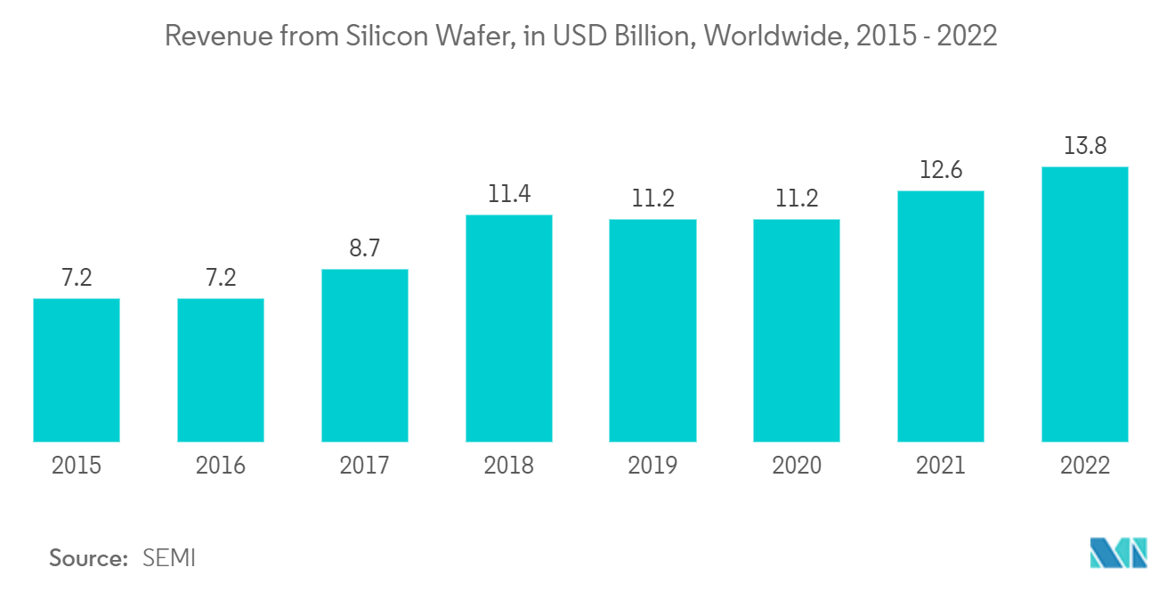
- The rise in the expansion of the wafer production plants will create an opportunity for the local and international wafer inspection players to develop new products according to the customer's requirements. For instance, according to SEMI, in 2022, the silicon wafer area shipments worldwide amounted to 14.71 billion square inches, which increased from 14.16 billion square inches in 2021. Silicon wafers are a vital building material for semiconductors, which indicates the usage of high-performance semiconductors in connected devices and driving the market. Further, in 2022, the total revenue from silicon wafers worldwide amounted to USD 13.8 billion, which increased from USD 12.6 billion, further indicating the market's growth.
Asia-Pacific to Dominate the Market
- The Asia-Pacific is one of the prominent regions for the semiconductor industry concerning manufacturing and consumption. According to SIA, Asia-Pacific is the largest regional semiconductor market, and China accounts for the most significant share in the region.
- Many regional companies are entering collaborations and partnerships in the semiconductor metrology/inspection equipment market. For instance, Shenzhen JT Automation Equipment, a Chinese chip production tool manufacturer, announced a legally binding five-year (2021-2025) memorandum of understanding with Huawei's HiSilicon Technologies business, China's largest chip developer. Both firms aim to expand their semiconductor packaging tool development partnership and create a self-sufficient and regulated industry.
- RTEC developed a new product, NovusEdge, for bare wafer edge and backside inspection. Edge die yield is becoming more critical as semiconductor manufacturing fabs attempt to save costs by reducing the wafer edge exclusion to produce a more significant number of yielding dies per wafer.
- Asia-Pacific has been a growing market for semiconductor equipment over the last few years. However, trade issues between the United States and China have presented uncertainty in the semiconductor metrology and inspection equipment market. Domestic semiconductor companies have been spending significantly to maintain their current market position by increasing their capacity and transitioning between technology nodes and wafer sizes. In the future, the demand is expected to be witnessed from the foundry in the region.
- In 2014, China's State Council proposed "National Integrated Circuit Industry Development Guidelines" to become a global leader in all semiconductor industry segments by 2030. Additionally, the Made in China 2025 initiative maintains achieving knowledge concerning advanced semiconductor manufacturing as a vital component of China's future economy and society. It is highly focused on the strategy to build a strong manufacturing nation worldwide.
- The initiative is expected to encourage local and foreign companies to invest in the Chinese market across various segments, including integrated circuits. The initiative prompts the government bodies to boost research and development activities so that China can rely on its own companies for core technologies rather than overseas ones. This is set to propel innovation in the semiconductor manufacturing industry.
Semiconductor Metrology & Inspection Equipment Industry Overview
The semiconductor metrology and inspection equipment market comprises prominent players such as Applied Materials Inc., Nikon Metrology NV, and KLA Corporation. These firms have continuously expanded their operation scales by focusing on market expansions and acquisitions. Acquisition activities effectively set the ball rolling regarding the overall market's growth in the market studied. Large companies have also been expending significant resources on R&D operations to protect their market position and drive innovation in the studied market shortly. Overall, the degree of competition remains high, primarily driven by the strong presence of prominent players involved in the market studied.
- July 2023: Applied Materials Inc. introduced materials, technologies, and systems that help chipmakers integrate chiplets into advanced 2.5D and 3D packages using hybrid bonding and through-silicon vias (TSVs). The new solutions will extend the company’s industry-leading breadth of technologies for heterogeneous integration (HI). The company is the largest supplier of technologies for HI with optimized chipmaking systems spanning etch, physical vapor deposition (PVD), chemical vapor deposition (CVD), electroplating, chemical mechanical polishing (CMP), annealing, and surface treatments.
- May 2023: KLA Corporation announced a strategic partnership with imec to develop the talent base and infrastructure to accelerate the advanced semiconductor applications for electrification and autonomous mobility and move the automotive industry forward. Through this partnership, both partners will bring relevant expertise to identify and manage programs aligned to the automotive industry, as well as talent development and recruitment.
Semiconductor Metrology & Inspection Equipment Market Leaders
KLA Corporation
Applied Materials Inc.
Onto Innovation Inc.
Thermo Fisher Scientific Inc.
Hitachi Hi-Technologies Corporation (Hitachi Limited)
*Disclaimer: Major Players sorted in no particular order
Semiconductor Metrology & Inspection Equipment Market News
- June 2023: Applied Materials Inc. announced the establishment of a collaborative engineering center in Banglore, India, focusing on developing and commercializing technologies for semiconductor manufacturing equipment. Through this center, the company aims to catalyze the training and development of future semiconductor industry talent and open new opportunities for India to play an expanded role in the global chip ecosystem.
- June 2023: ThermoFisher Scientific Inc. announced the introduction of a new generation, fully automated (S)TEM metrology solution for increased productivity and data quality assurance in semiconductor manufacturing. This solution is designed to meet an industry need for faster access to large-volume and high-quality data, and it aims to optimize performance and reduce operating expenses.
Semiconductor Metrology & Inspection Equipment Market Report - Table of Contents
1. INTRODUCTION
1.1 Study Assumptions and Market Definition
1.2 Scope of the Study
2. RESEARCH METHODOLOGY
3. EXECUTIVE SUMMARY
4. MARKET INSIGHTS
4.1 Market Overview
4.2 Industry Attractiveness - Porter's Five Forces Analysis
4.2.1 Bargaining Power of Suppliers
4.2.2 Bargaining Power of Buyers
4.2.3 Threat of New Entrants
4.2.4 Threat of Substitutes
4.2.5 Degree of Competition
4.3 An Assessment of the Impact of Key Macro Trends
5. MARKET DYNAMICS
5.1 Market Drivers
5.1.1 Increasing Demand for High-performance, Low-cost Semiconductors
5.1.2 Increasing Demand for Semiconductor Wafers in Consumer Electronics
5.2 Market Restraints
5.2.1 High Setup Cost and Lack of Expertise in Handling Metrology Systems Efficiently
5.2.2 High Raw Material and Fabrication Costs
6. MARKET SEGMENTATION
6.1 By Type
6.1.1 Lithography Metrology
6.1.1.1 Overlay
6.1.1.2 Dimension Equipment
6.1.1.3 Mask Inspection and Metrology
6.1.2 Wafer Inspection
6.1.3 Thin Film Metrology
6.1.4 Other Process Control Systems
6.2 By Geography
6.2.1 North America
6.2.2 Europe
6.2.3 Asia-Pacific
6.2.4 Rest of the World
7. COMPETITIVE LANDSCAPE
7.1 Company Profiles
7.1.1 KLA Corporation
7.1.2 Applied Materials Inc.
7.1.3 Onto Innovation Inc.
7.1.4 Thermo Fisher Scientific Inc.
7.1.5 Hitachi Hi-Technologies Corporation (Hitachi Limited)
7.1.6 Nova Measuring Instruments Ltd
7.1.7 ASML Holding NV
7.1.8 Lasertec CorporatioN
7.1.9 JEOL Ltd
7.1.10 Nikon Metrology NV (Nikon Group)
7.1.11 Camtek Limited
- *List Not Exhaustive
8. INVESTMENT ANALYSIS
9. FUTURE OF THE MARKET
Semiconductor Metrology & Inspection Equipment Industry Segmentation
Semiconductor metrology and inspection are essential for the management of the semiconductor manufacturing process. There are 400 to 600 steps in the manufacturing process of semiconductor wafers, which are undertaken in one to two months. If deficiencies occur early in the process, all the work undertaken in the subsequent time-consuming steps will be wasted. Metrology and inspection processes are established at critical points of the semiconductor manufacturing process to ensure that a specific yield can be confirmed and maintained.
The semiconductor metrology and inspection equipment market is segmented by type (Lithography Metrology (Overlay, Dimension Equipment, Mask Inspection, and Metrology), Wafer Inspection, and Thin Film Metrology), geography (North America, Europe, Asia-Pacific, and Rest of the World). The market sizes and forecasts are provided in terms of value in USD for all the above segments. The competitive landscape has been taken to calculate the penetration of semiconductor metrology and inspection equipment and how players involve themselves in organic and inorganic growth strategies. Companies continuously innovate their products to increase their market share and profitability. Furthermore, the market study focuses on the impact of key macro trends on the market ecosystem.
| By Type | |||||
| |||||
| Wafer Inspection | |||||
| Thin Film Metrology | |||||
| Other Process Control Systems |
| By Geography | |
| North America | |
| Europe | |
| Asia-Pacific | |
| Rest of the World |
Semiconductor Metrology & Inspection Equipment Market Research FAQs
What is the study period of this market?
The Semiconductor Metrology And Inspection Equipment Market is studied from 2018 - 2028.
What is the growth rate of Semiconductor Metrology And Inspection Equipment Market?
The Semiconductor Metrology And Inspection Equipment Market is growing at a CAGR of 5.2% over the next 5 years.
What is Semiconductor Metrology And Inspection Equipment Market size in 2018?
The Semiconductor Metrology And Inspection Equipment Market is valued at 9 Billion USD in 2018.
What is Semiconductor Metrology And Inspection Equipment Market size in 2028?
The Semiconductor Metrology And Inspection Equipment Market is valued at 12 Billion USD in 2028.
Which region has highest growth rate in Semiconductor Metrology And Inspection Equipment Market?
Asia Pacific is growing at the highest CAGR over 2018 - 2028.
Which region has largest share in Semiconductor Metrology And Inspection Equipment Market?
Asia Pacific holds highest share in 2022.
Who are the key players in Semiconductor Metrology And Inspection Equipment Market?
KLA Corporation, Applied Materials Inc., Onto Innovation Inc. , Thermo Fisher Scientific Inc., Hitachi Hi-Technologies Corporation (Hitachi Limited) are the major companies operating in Semiconductor Metrology And Inspection Equipment Market.
Semiconductor Metrology & Inspection Industry Report
Statistics for the 2023 Semiconductor Metrology & Inspection market share, size and revenue growth rate, created by Mordor Intelligence™ Industry Reports. Semiconductor Metrology & Inspection analysis includes a market forecast outlook to 2028 and historical overview. Get a sample of this industry analysis as a free report PDF download.